Designing a high-speed printed circuit board (PCB) requires careful consideration of various factors to ensure signal integrity and performance. Here are the top 10 tips for high-speed PCB design:
Layer Stackup Optimization:
Plan your PCB stack up carefully. Use controlled impedance layers for high-speed signal traces to maintain signal integrity. Properly place power and ground planes to minimize noise and provide return paths for signals.
Signal Integrity Analysis:
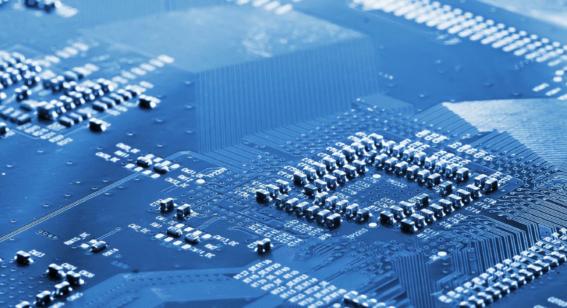
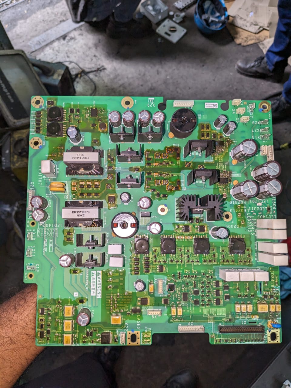
From Google Photos
Perform signal integrity analysis using simulation tools like SPICE or field solvers to identify potential signal integrity issues, such as reflections, crosstalk, and impedance mismatches.
Keep Traces Short:
Minimize trace lengths to reduce signal propagation delay and signal degradation. Use vias and layer changes judiciously, and route critical signals directly, avoiding unnecessary bends and detours.
Impedance Matching:
Ensure that the characteristic impedance of high-speed traces matches the impedance of the source and load components. This helps prevent signal reflections and improves signal quality.
Differential Pair Routing:
For high-speed differential signals (e.g., USB, HDMI, PCIe), route the positive and negative signals close together to maintain their balance and reduce common-mode noise.
Decoupling and Bypassing:
Place decoupling capacitors near the power pins of ICs to provide a low-inductance path for high-frequency currents and to reduce noise on the power supply lines.
Ground Plane Design:
Create a solid ground plane to provide a low-impedance return path for signals. Avoid splitting the ground plane underneath high-speed traces to minimize return path discontinuities.
Minimize Crosstalk:
Keep sensitive signals away from high-speed or noisy traces. Use isolation techniques like guard traces or spacing to reduce crosstalk between adjacent signals.
Thermal Considerations:
High-speed circuits can generate heat. Adequately dissipate heat using thermal vias and proper placement of heat-generating components. Consider the operating environment and thermal management requirements.
Design for Manufacturability (DFM):
Consider DFM guidelines early in the design process. Ensure that your high-speed design is manufacturable and cost-effective. Review manufacturing capabilities and limitations with your PCB fabrication and assembly vendors.
Bonus Tip: EMC/EMI Considerations:
To avoid electromagnetic interference (EMI) issues, design your high-speed PCB with good electromagnetic compatibility (EMC). Use proper shielding and grounding techniques as needed.
Remember, high-speed PCB design is a complex task that requires a deep understanding of electrical principles and PCB layout techniques. Simulation and analysis tools are invaluable for verifying your design before fabrication. Always collaborate with experienced PCB designers or engineers to optimize your high-speed designs.
