Huawei has claimed a 1.4nm-equivalent transistor density without access to ASML’s EUV lithography systems. If that claim holds up, it would be a major result, but it would not mean Huawei has fabricated a true 1.4nm process node.
The important story is 3D chip design. Huawei says it can stack and connect logic in ways that shrink the time data spends moving across a processor. Yet the numbers remain company-provided, with no independent benchmarks or mass-production evidence so far.
The distinction between a denser chip and a smaller transistor is where this story begins.
Table of Contents
Why the TSMC 1.4nm Chip Comparison Draws So Much Attention
Huawei’s claim attracts attention because it appears to put a sanctioned company near the density associated with leading manufacturers such as TSMC. However, process-node names no longer work as simple measurements of transistor size. A so-called 2nm chip does not contain transistors that are precisely 2 nanometers wide, and a 1.4nm-equivalent density does not prove a manufacturer has built a true 1.4nm node.
The comparison matters because Huawei has faced limits that TSMC has not. ASML’s EUV lithography systems print the most demanding layers in advanced chips at high volume. Huawei has been blocked from buying that equipment, so it and Chinese foundry SMIC have had to pursue other routes.
DUV pushed further through multiple patterning
Older deep ultraviolet, or DUV, lithography has lower resolution than EUV. Manufacturers can compensate by splitting one complex pattern into several exposure and etching steps. This technique, called multiple patterning, can create finer features than a single DUV exposure could produce.
The tradeoff is severe. Each added patterning step raises cost, introduces alignment risk, and creates more chances for defects. ASML has described how EUV can replace several DUV patterning steps for certain layers, which reduces opportunities for patterning errors in its comparison of DUV and EUV.
Huawei’s reported approach does not remove those manufacturing pressures. Instead, it tries to get more out of mature lithography by changing the architecture of the chip.
Moore’s Law no longer delivers easy gains
Moore’s Law began as an observation that transistor counts could roughly double over time. For decades, shrinking transistors made chips denser, faster, and more efficient at a pace that shaped the entire electronics industry.
That formula has become harder to sustain. Each new generation needs more expensive tools, tighter process control, and years of development. Even past lithography transitions required clever workarounds, as ASML recounts in its history of immersion lithography and Moore’s Law.
Silicon’s physical limits are part of the problem. Components cannot shrink indefinitely when their dimensions approach the scale of atoms and quantum effects become harder to control.
A smaller transistor does not always create a faster chip
A modern processor is not only a field of transistors. It is also a maze of metal interconnects that carry signals between those transistors, memory, caches, and control circuits.
Every wire has resistance, which slows a signal, and capacitance, which requires energy to charge and discharge. Together, those effects create RC delay. As transistors switch faster, wire delays can become the larger obstacle.
In advanced chips, speed can depend more on the distance data travels than on the switching speed of a single transistor.
This helps explain why many mobile processors have remained near the 3 to 4 GHz range even as transistor counts continue to rise.
How Huawei’s Logic Folding and Tau Scaling Could Make Chips Faster
Huawei calls its reported approach “tau scaling,” using tau as a symbol for time. The goal is to reduce signal travel time rather than relying only on smaller transistors on a flat die.
Its related concept, “logic folding,” places connected blocks of processor logic above and below each other. A chip that spreads those blocks across a wide silicon surface may force signals to cross long horizontal paths. A vertically designed chip could move some of those paths upward through tightly spaced connections.
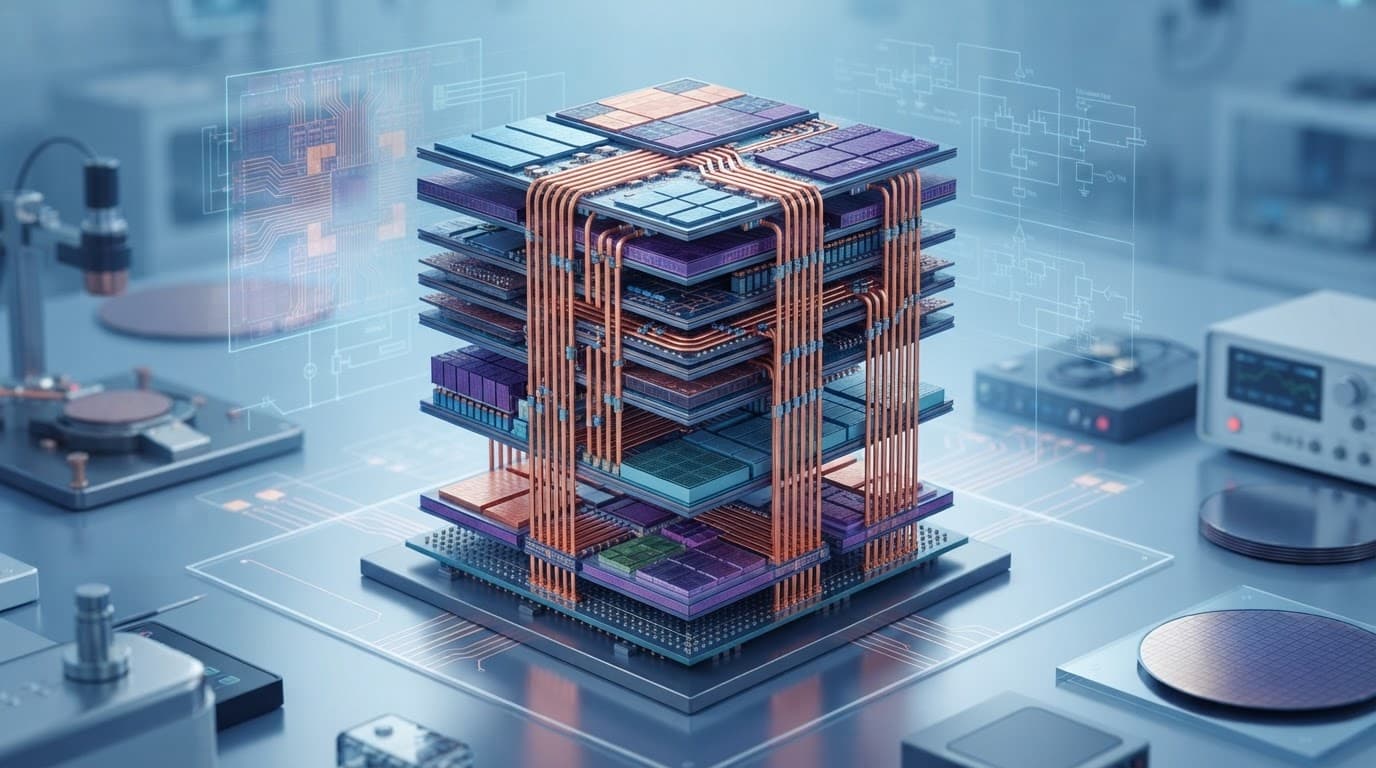
A folded sheet of paper offers a useful visual. Two points that began far apart become neighbors once the sheet folds. Huawei proposes to apply that geometry to processor logic.
Logic folding starts during chip layout
Chips already use vertical technology. High-bandwidth memory, or HBM, stacks multiple memory dies. AMD’s 3D V-Cache places cache memory above processor logic. Chiplets also bring separately made dies together in a single package.
Huawei’s claim differs in where the vertical design begins. Standard 3D packaging often joins dies that engineers designed as separate flat chips. Logic folding, as presented by Huawei, would identify the processor’s slowest timing paths during layout and distribute related logic across multiple layers from the start.
That matters because the placement of each vertical connection affects timing, power delivery, testing, and heat flow. The architecture has to treat the stack as one processor, not a pile of finished components.
Why a 1.5-micron bonding pitch matters
Huawei has claimed a hybrid-bonding pitch of about 1.5 to 2 microns. This measurement is not the transistor size. It is the distance between the vertical copper-to-copper contacts that connect stacked silicon layers.
A smaller pitch allows more connections in the same space. Those contacts must also sit close to the logic blocks that need them. Otherwise, a signal still wastes time traveling sideways to find a path up or down.
Huawei compared its target with 3D logic examples around 9 to 10 microns, including AMD’s 3D V-Cache. If a 1.5-micron pitch is repeatable at high yield, it could allow separate logic layers to operate more like one unified die. That claim needs proof at production scale.
What the reported Kirin numbers suggest
Huawei’s presentation describes a previous design at roughly 155 million transistors per square millimeter, then projects about 238 million for a Kirin 2026 design using logic folding. It compares that figure with an estimated 236 million transistors per square millimeter for TSMC’s N2 process.
The company also claims a 60% reduction in average data-travel distance, 25% lower signal latency, fewer clock buffers, and a 3.1 GHz performance core. Each figure comes from Huawei’s presentation and remains unverified.
Those numbers describe a possible architectural gain, not proof that Huawei has matched every part of a TSMC N2 chip. Performance, power draw, yields, software support, and thermal behavior all remain open questions.
The Engineering Problems That Could Stop a Vertical Chip Plan
A dense design on a presentation slide is not yet a reliable smartphone processor. Huawei’s plan depends on manufacturing, design software, and cooling systems that can support a far more tightly packed arrangement of active logic.
EDA software was built for flat chips
Electronic design automation, or EDA, tools have spent decades optimizing two-dimensional circuit layouts. They must now account for vertical placement, inter-layer timing, power delivery, signal interference, test access, and manufacturing limits.
A 3D layout cannot simply take a flat design and add another floor. Designers must know whether a critical path remains fast after it crosses layers. They also need to model how power moves through the stack and how heat changes the behavior of nearby transistors.
Huawei has acknowledged that its framework for this work is still developing. Even excellent bonding technology would take time to reach products if design software cannot reliably create and verify the chips.
Stacked active logic creates a heat problem
Memory stacks are difficult enough, but active logic generates much more heat because it switches constantly. A stack of processor layers concentrates that activity in a small volume, while the middle layers sit farther from the phone’s cooling surfaces.

A data center can use large heat sinks, fans, liquid cooling, and generous power budgets. A phone has a thin chassis, a battery nearby, and little room for heat to escape. If temperatures rise too far, the processor must throttle its clock speed. That can erase much of the promised performance gain during long gaming sessions, video work, or AI tasks.
Thermal management is therefore one of the most important tests of Huawei’s roadmap.
Yield, testing, and repair get harder in three dimensions
Huawei has suggested near-perfect manufacturing yield for its bonding approach. That would be an exceptional result, but only high-volume production can confirm it.
In a stacked design, a defect in either bonded layer can ruin the whole assembly. Dense contacts also complicate inspection because many structures are buried inside the stack. Testing has to find weak links, timing failures, and power problems before a chip reaches a phone.
Factory automation will matter here as much as lithography. Modern semiconductor production depends on high-speed inspection, precision handling, data analysis, and process control, all themes shaping smart manufacturing in 2026.
A 1.4nm-Equivalent Density Is Not a True 1.4nm Process
The short answer is no. Huawei’s 1.4nm-equivalent language refers to a density result that could come from placing multiple mature-node layers into a smaller three-dimensional volume.
A true next-generation node also involves the transistors themselves. It includes switching speed, leakage current, power efficiency, transistor structure, wiring rules, process control, and the ability to manufacture at commercial yields.
Density, speed, power, and node names measure different things
Transistor density measures how many transistors fit within an area. Volume density can rise further when a manufacturer stacks layers. Clock speed measures cycles per second, while energy efficiency depends on how much power a chip uses to complete work.
A process-node name combines many characteristics and also carries marketing history. It is not a universal ruler. Huawei could potentially match an N2-class density figure through stacking while using transistors that are less efficient or slower than those in a leading-edge N2 process.
That does not make 3D integration unimportant. It means readers should separate a density comparison from a full process-node comparison.
What would confirm Huawei’s claims
The claims need evidence that survives outside a company presentation. The most useful proof points would include:
- Independent die photographs and analysis of the physical layer structure.
- Sustained benchmark scores rather than brief peak results.
- Measured power draw, heat output, and battery life in finished phones.
- Production volumes and repeatable yield data across many units.
- Performance after long workloads, when thermal throttling becomes visible.
Store-shelf hardware matters most because it forces every part of the system to work together. A chip can look dense and fast in a controlled demo, yet still struggle with heat, battery life, or manufacturing consistency.
What This Could Mean for TSMC, Intel, and Chip Design
Huawei did not invent vertical chip integration. TSMC, Intel, AMD, and other companies already invest heavily in advanced packaging, chiplets, hybrid bonding, and 3D memory. The semiconductor industry has been moving toward system-level designs because shrinking a flat transistor alone no longer solves every performance problem.
Huawei’s situation adds urgency. Export restrictions may have pushed it to search for gains that do not require the newest EUV equipment, while companies with EUV access can combine smaller transistors with similar 3D techniques.
Could vertical design narrow the gap?
Logic folding could reduce some disadvantages created by older lithography. Shorter signal paths may improve certain workloads, and higher effective density can fit more functionality into a compact package.
Still, a single claimed chip cannot prove that China has closed the semiconductor gap with TSMC or Intel. Leading manufacturers have advantages in equipment access, materials, manufacturing capacity, EDA ecosystems, packaging, and years of yield learning.
Huawei’s proposal should be viewed as a possible route around one bottleneck, not a complete substitute for the entire advanced-chip supply chain.
Future gains may center on nanoseconds, not nanometers
The strongest idea in Huawei’s presentation is not the 1.4nm label. It is the focus on time. When data moves shorter distances, processors can spend less energy waiting on wires, buffers, and long routing paths.
Future chips may combine smaller transistors with chiplets, on-package memory, dense hybrid bonding, and vertically arranged logic. In that future, the classic flat processor becomes only one part of the design.
A high-performance motion controller offers a smaller-scale example of the same demand: processors increasingly need to handle logic, data, and real-time work near the point where decisions occur. Faster connections between compute elements matter across phones, servers, and industrial systems.
The Claim Needs Silicon, Not Slides
Huawei’s logic-folding concept addresses a real problem. Wire delay, not transistor switching alone, has become a stubborn limit on modern chip performance. Dense vertical connections could reduce that delay and make mature process technology more useful than many people expected.
However, 1.4nm-equivalent density should not be confused with a true 1.4nm manufacturing node. Huawei must still prove usable design tools, safe thermal performance, and repeatable high-yield production.
Independent benchmarks and commercially available Kirin hardware will show whether this is a durable advance in 3D chip architecture or an ambitious roadmap waiting for its hardest tests.